19:17
Sony Alpha Cameras Powering a New Eye Test and Digital Eyewear Shop
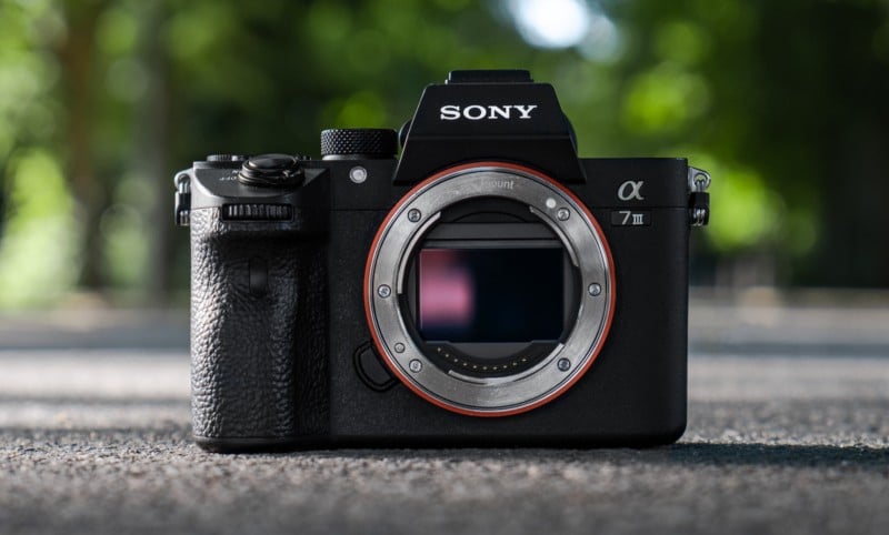
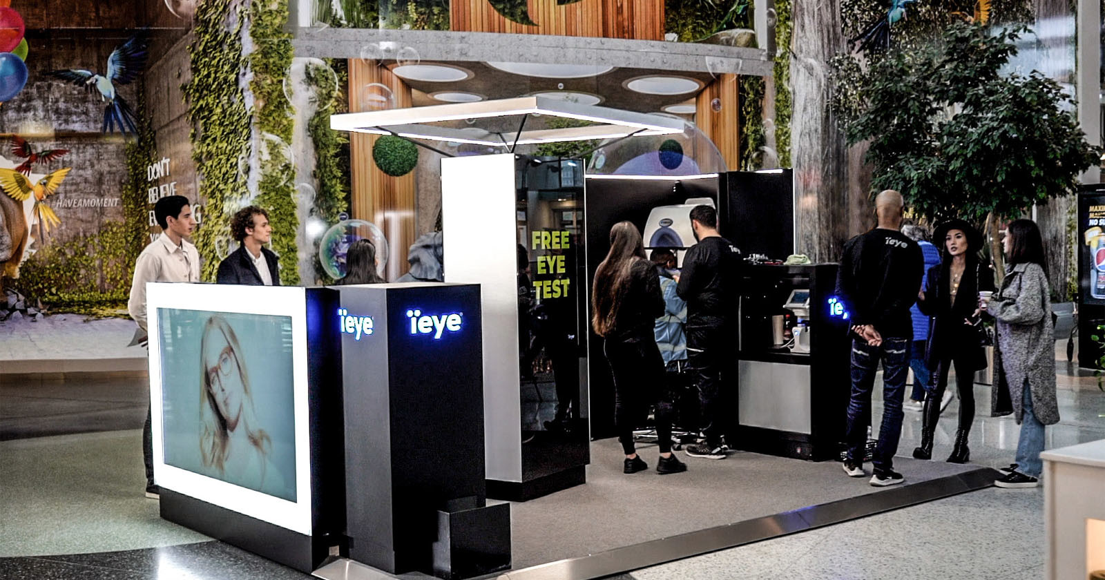
Swedish tech company ieye has partnered with Sony in a new kiosk that uses an Alpha camera to scan a shopper's face to provide a bespoke selection of frames tailored specifically to an individual. [Read More]