ФОТО: petapixel.com
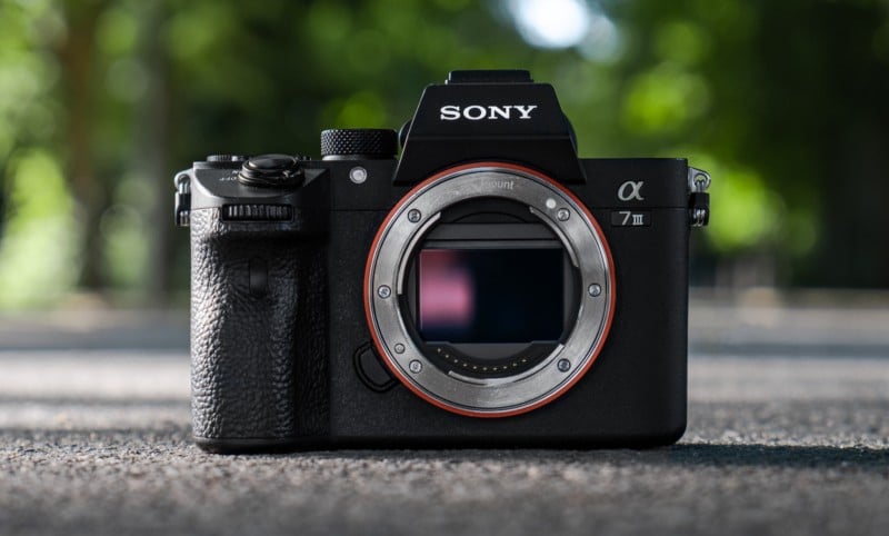
Sony has showcased a first-look inside its Osaka Office, which is dedicated to CMOS image sensor development and has been designed by the engineers who work there to cultivate a positive and stimulating work environment that breaks from traditional Japanese corporate structure.
First launched in April 2020, the Osaka Office is the center for Sony […]. petapixel.com
2021-6-2 23:38